- The world's
- advanced storage
- solutions
-
Adopt outstanding technology and innovative development, to provide large capacity, high performance, reliable and durable storage devices.
Controller & Firmware
Autonomous Control
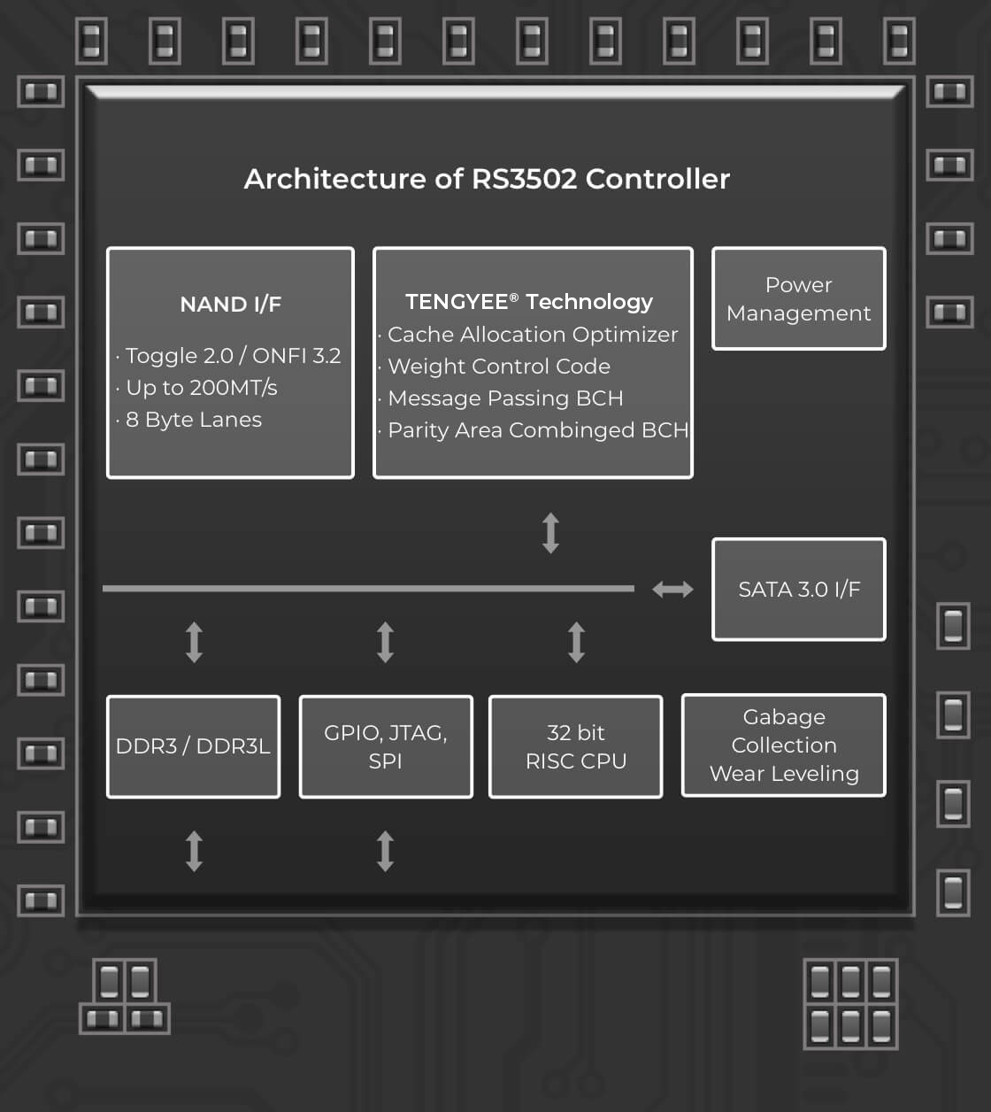
RS3502 Controller – Independent R&D, Focus on industrial Field
-
AES EncryptionIn-built 256bit AES encryption,enable for various encryption and erase technology
-
500 MB/sSequential performance up to 500MB/s
-
64 CEDesign with dual 32bit processor, 8 lanes 64CE NAND channels
-
FirmwareOptimize flash management according to industrial and industrial application scenarios
-
80 BIT/1KBEach lane supports 8CENAND and super ECC ability to 80bit/1KB
-
DDRSupport external DDR
Exclusive technology
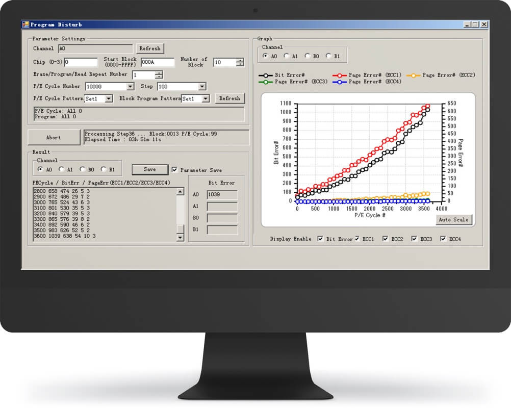
Powerful ECC Capability to Extend Lifespan of NAND Flash
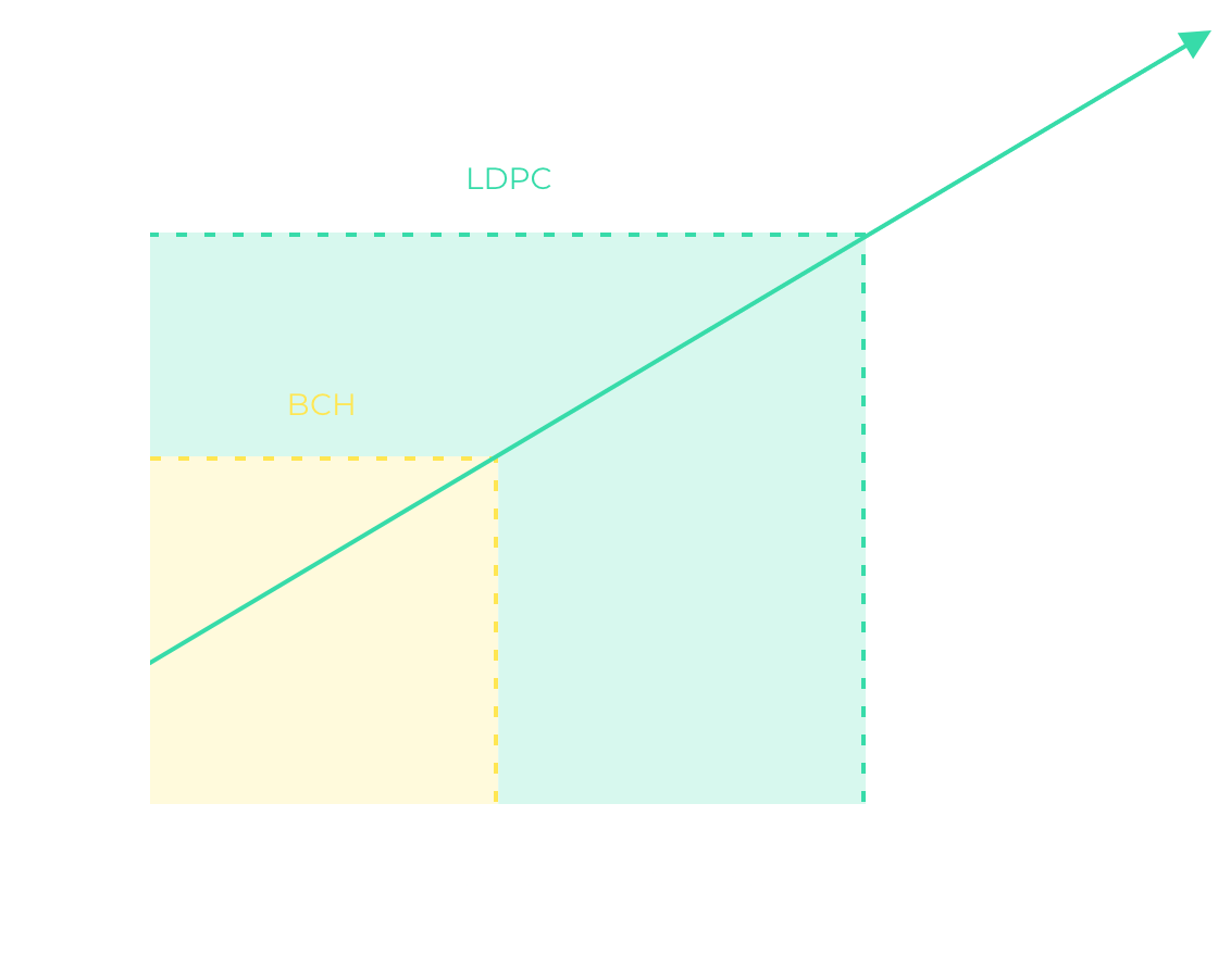
Test Result of
Renice ECC & Normal ECC


No Trim-Full Speed Performance
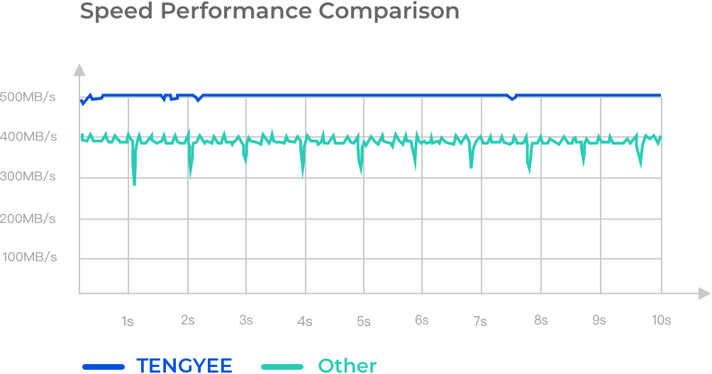
Global Unique Technology
Non-Balance Wear Leveling TechnologyTM
Renice Non-Balance algorithm idea as: An able man is always busy
According to the actual P/E Cycle, the ability to achieve more.
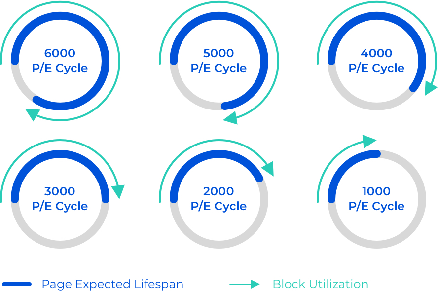
To extend lifespan via converting NAND mode based on the error threshold rate
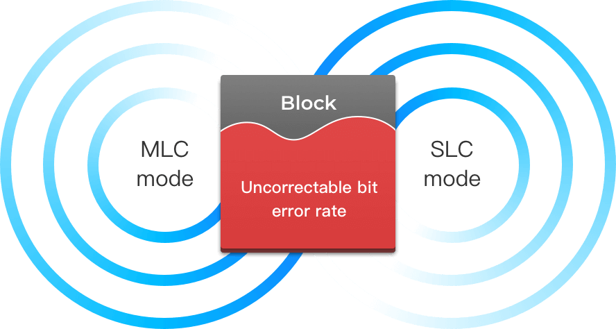
MLC to SLC Technology
Stable Performance
PR-Latency Garbage Collection Technology
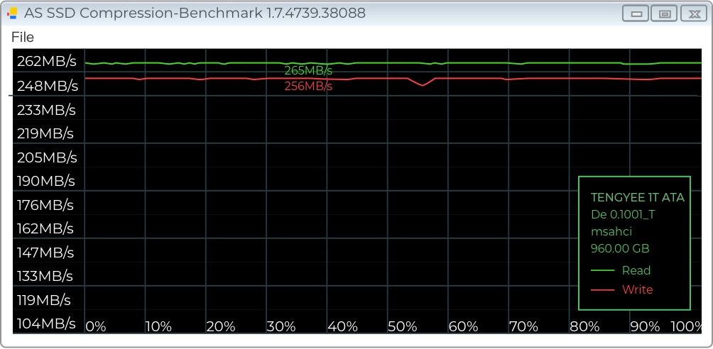
Performance not less than
80%
Proprietary technology
r-Backup Power Failure Protection
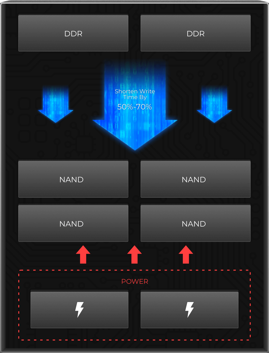
Shorten Write Time by
50%-70%
300,000 times Abnormal Power-off Test
0 Defect
Customize Special Functions
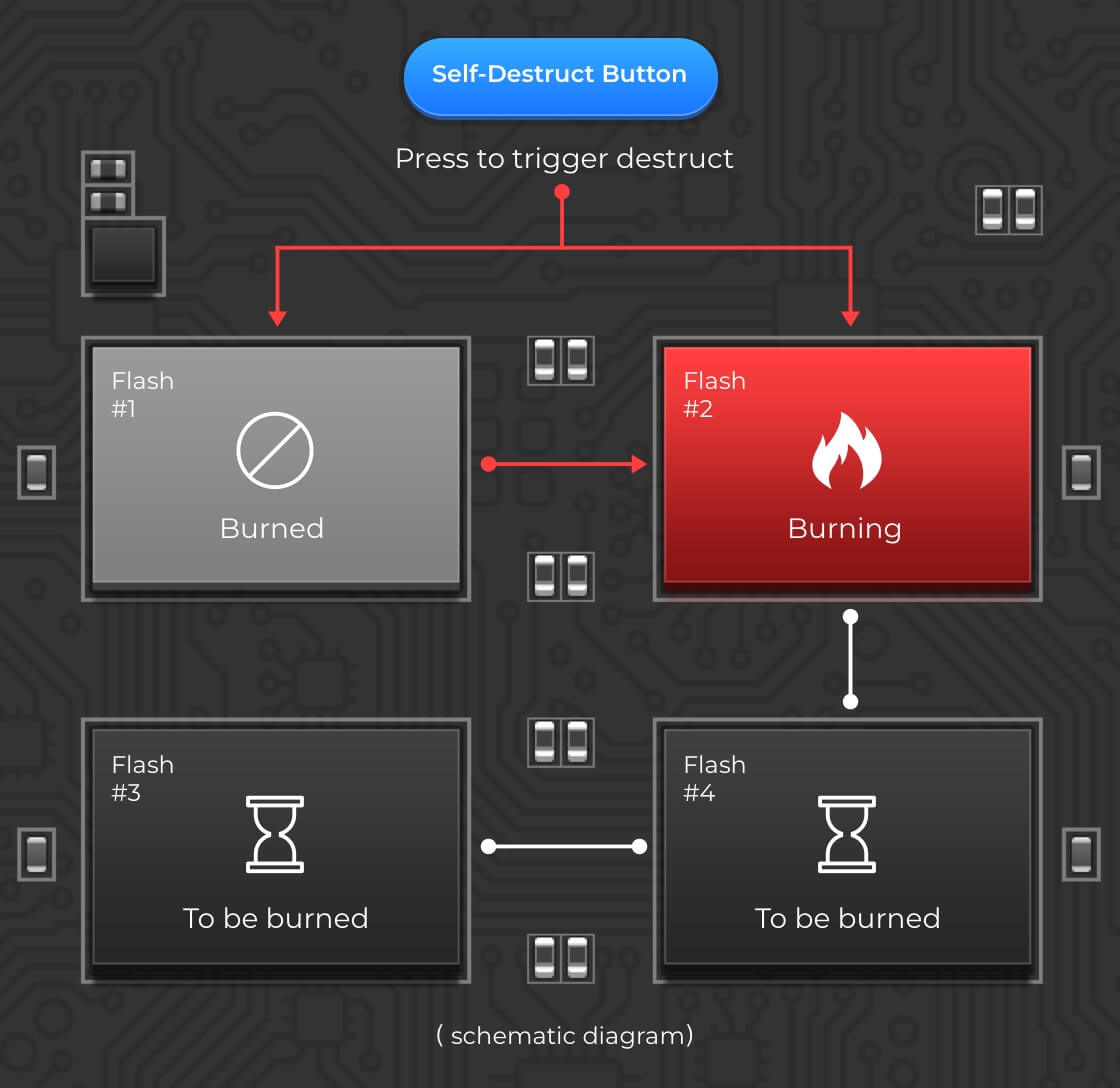

Time-sharing Shunt
Burndown flash chips one by one by means of time-sharing shunt design, ensure all flash chips are destroyed

Burn-down in 100ms
Ensure to burn down the flash chips completely within 100ms. The burning time of entire SSD is adjustable

High Voltage Breakdown
Breakdown the flash chips through high voltage thoroughly to avoid data been recovered

Real-time Feedback
Unique circuit to achieve real-time monitoring of burning status.

5s False Triggering
Default with 5s false trigger time after power on. The time is adjustable.

False Trigger Prom
There will be warning lights when pressing destruct button in state of power-off
Exclusive technology
SSD Data Destruction Methods in industrial Applications

Physical Space Displacement
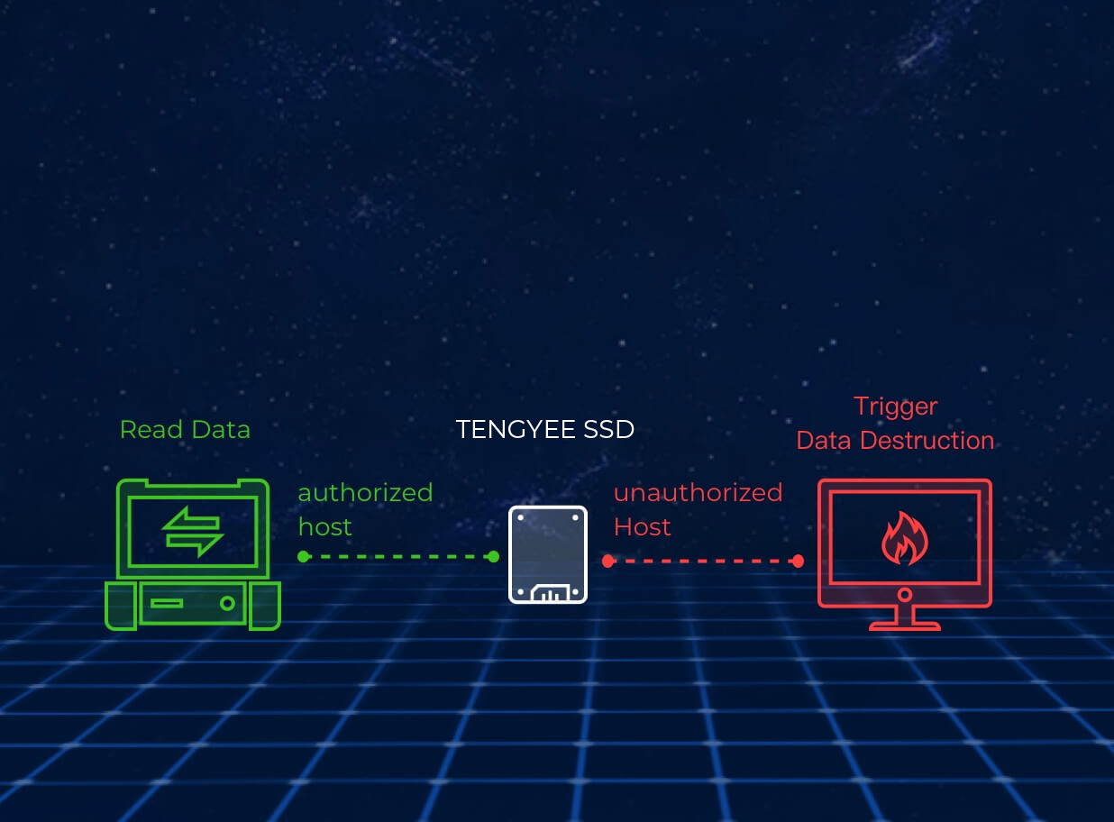
Connected with unauthorized Host
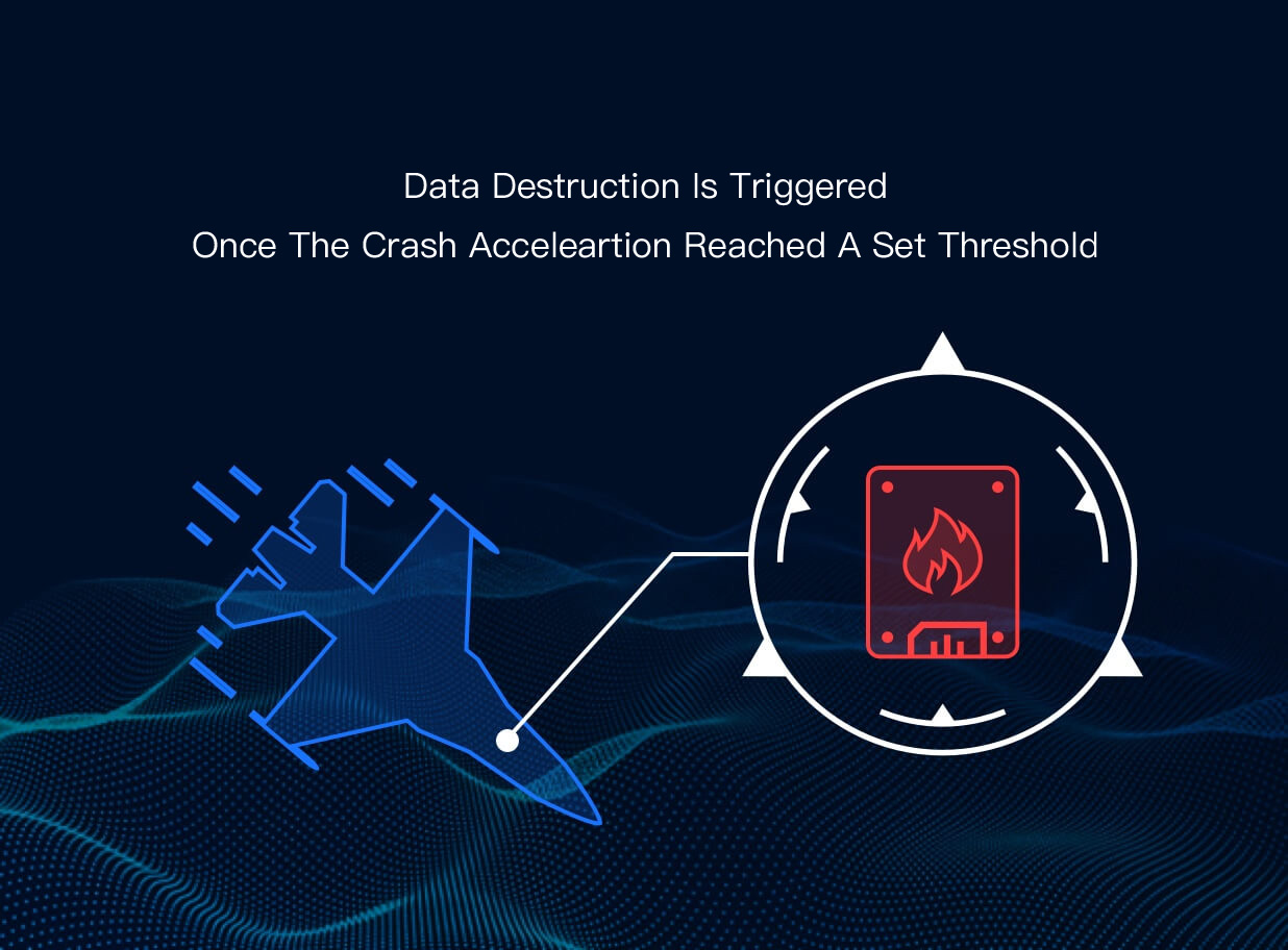
Acceleration Induction
Independent development
High Reliable Rugged SATA Connector
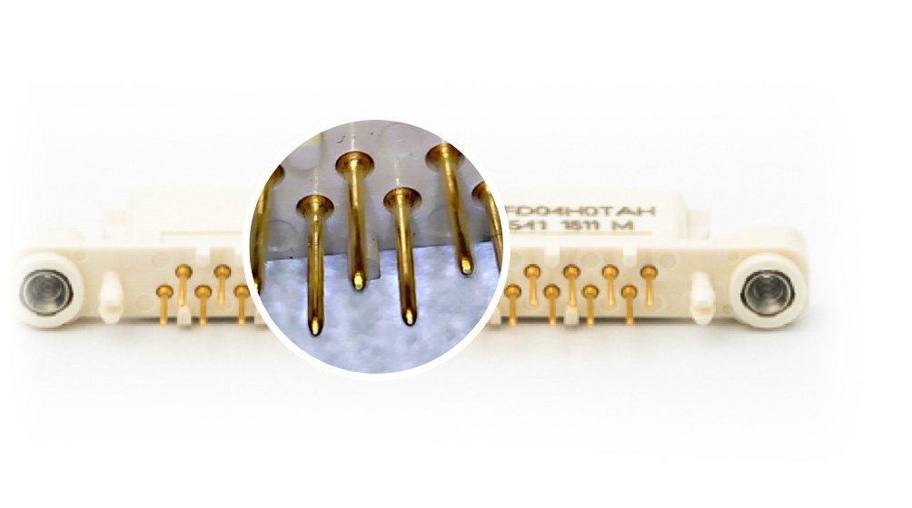
Strong Buffer Design
The rugged connector with special buffer structure between connector and PCB. Each Pin is designed with spherical at the bottom, to ensure rotation at the same angle and maximize the buffer effect in face of strong shock and vibration, therefore to avoid damage of connectors.
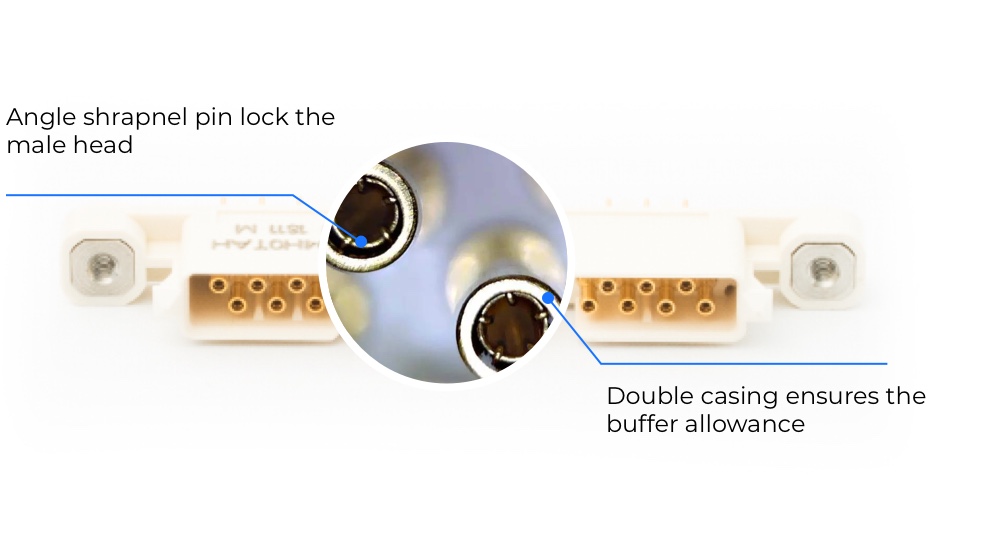
Mother Connector designed with Double Casing
Take into account of simple-swap, no poor contact and not damage the Pin, the mother-connector is designed with double casing to provide enough buffer. And the inner 5 spring strip guarantee full contact with male connector perfectly.
Independent development
Software Encryption

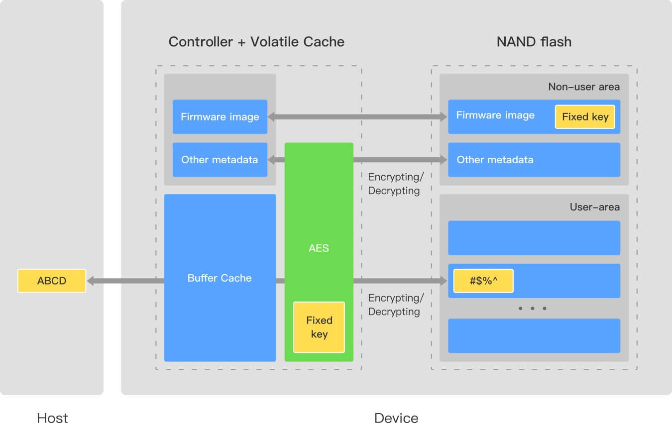
AES Encryption
Perform Data Secure Erase under power failure
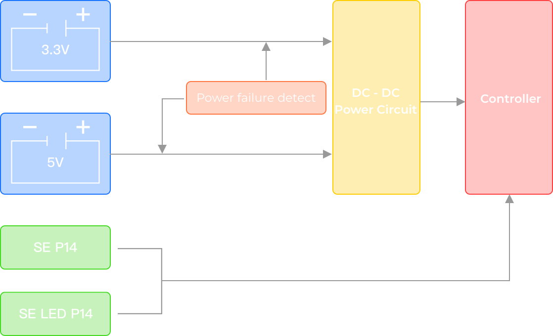
Secure Erase under Power Failure
High Specification Production Process
Exclusive process
industrial Grade Materials, Strict Production Process
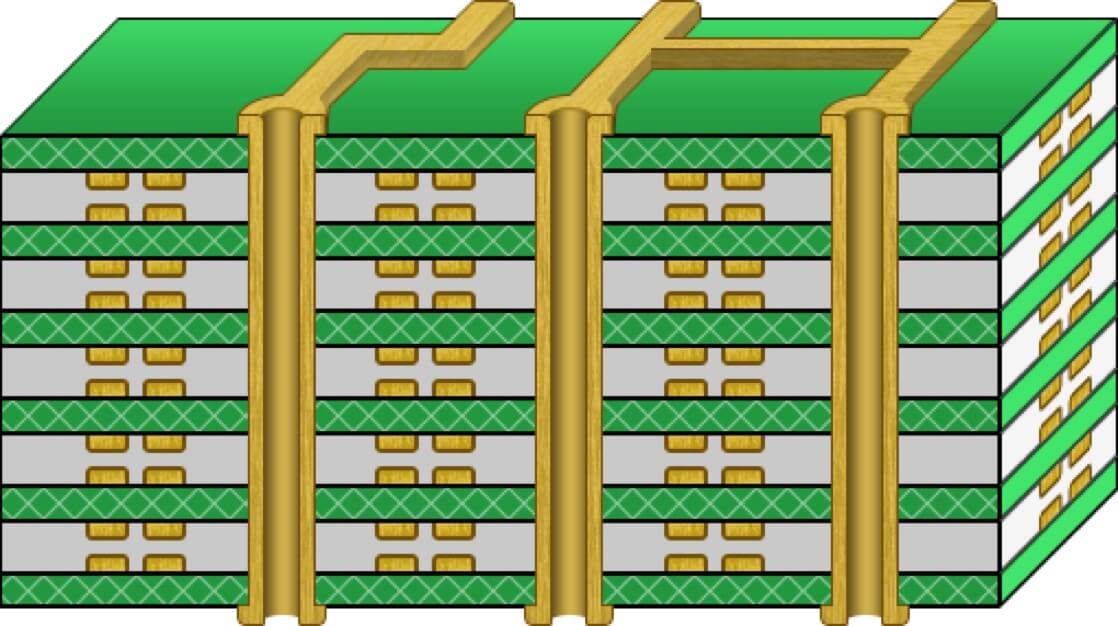
industrial Standard PCB
Conformal Coating Technology
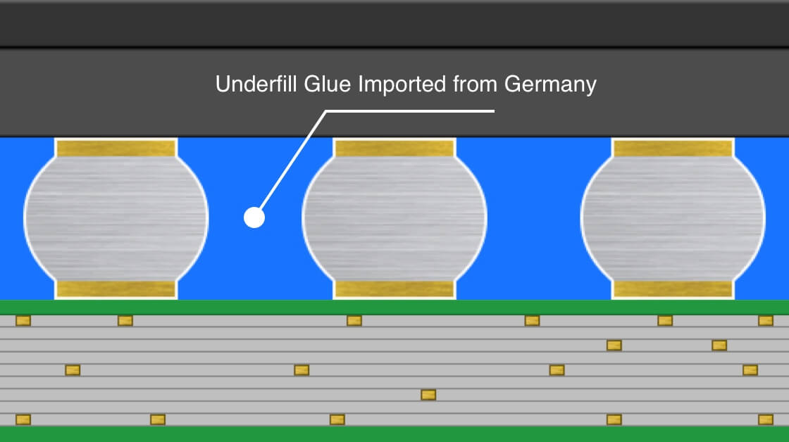
Chips Reinforcement Technology
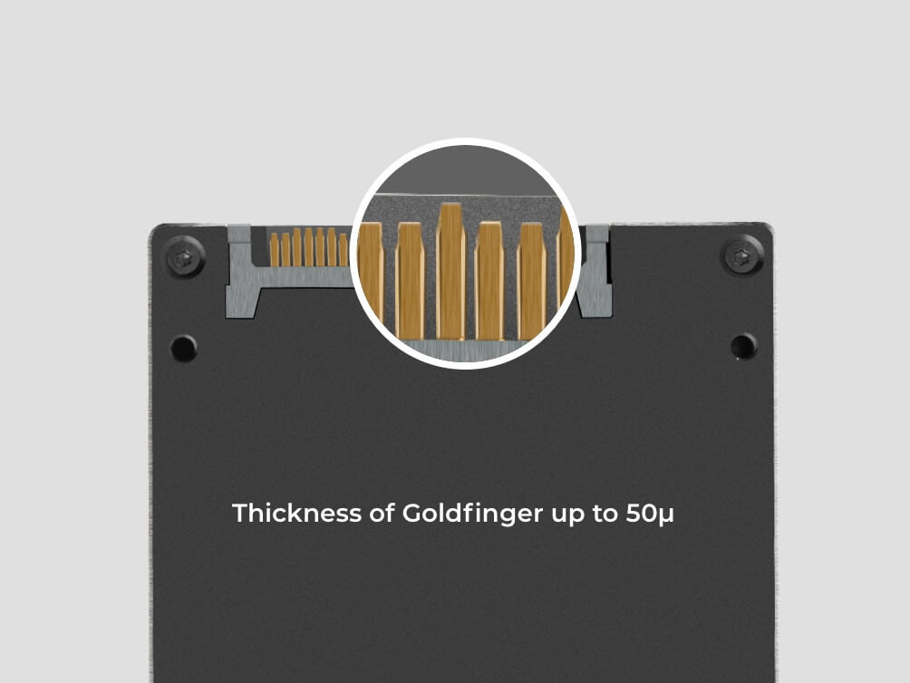
Key Processes
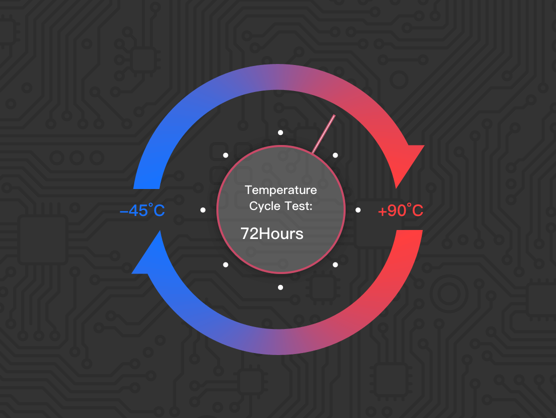
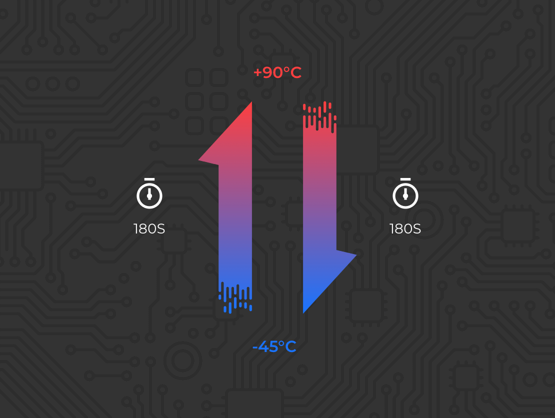
Strict High-Low Temperature Test
Temperature Cycle Test:
 Products
