Root Cause Analysis & Test for NAND Flash Bit Error
Bit Error is an inevitable phenomenon talking from the physical structure of NAND Flashes. Being impacted by the working environment (e.g. Temperature, Irradiation), production workmanship, working principle and the disadvantages of the memory material itself, NAND flashes are always hard to avoid error. Error Rate indicates the rate of error produced in certain conditions; it reflects the present reliability status of the NAND Flash.
The Physical Root of Errors
Cell is a MOS type transistor of Floating Gate (FG as the abbreviation) structure, it works with the principle of changing the threshold voltage by injecting or releasing electric charge to FG to achieve the goal of storing or deleting data. Program “0” injects electric charge into FG by applying voltage through Control Gate, while the erasing process is applying reverse voltage to pull out the electric charge through Fowler Nordheim Tunneling (FNT), FNT may cause random electrical noise due to energy-trap capture or electron leakage from the single-layer oxide near the surface of the base plate, such noise finally cause threshold voltage excursion.
With the development of NAND Flash manufacturing processing, the HalfPitch between FGs is getting smaller and smaller in a rapid pace from the 360nm in 1995 to today’s 16nm. Such workmanship which compresses CMOS constantly because of the advancing manufacturing processing causes multiple impacts to NAND flash reliability, e.g. The quantity of electric charge in FG decreased, there are about 100 electrons stored in a FG of 34nm, the charge loss tolerance is 10 electrons, while there is only about 10 electrons in a FG of 19nm, therefore losing any single electron will cause significant impact to threshold voltage. The closer distance can also bring easier affection between memory cells. Besides, Time dependent dielectric breakdown (TDDB) or dielectric fatigue will happen to FG under the influence of voltage and electric field, thus lead to Bit Error.
The Erase and Program operations also leads to charge collection by oxide layer, this will affect the threshold voltage of cell, threshold voltage shift due to charge detrapping causes Bit reverse.
Plastic-encapsulation process is also a hazard causing errors. NAND Flash mainly adopts plastic-encapsulated circuit, the plastic-encapsulation process may face the problems such as moisture absorption, layering, hot conduction, cavity. Therefore, those strictly operated factories often bake the NAND Flashes before SMT to avoid fracture or surface bubbles to the chipsets caused by heating after absorbing moisture. Although the fracture of chipset is the most serious problem, the damage of internal physical structure is also a safe hazard.
Bit Error Symptoms
Bit error occurs in below cases:
1. P/E Cycle
2. Read Disturb
3. Program Disturb
4. Data Retention error
Read/Program Disturb mainly occurs when read/write operation to the target Cell brings affects to the adjacent Cells with changing their threshold voltage or Electric field, thereby causes data errors to the adjacent Cells.
While Data Retention Error is caused by the increasing number of remaining electrons brought by oxide layer or shifting threshold voltage of Cell by electric leakage . Please refer to the following part “Data Retention” for detail info.
Bit Error Rate Test Method
Bit Error Rate is usually expressed as RBER(Raw Bit Error Rate) and UBER(Uncorrectable Bit Error Rate). RBER represents the Bit Error Rate before ECC correction, it reflects the initial reliability state of the NAND flash. UBER indicates the Bit Error Rate in ECC with a certain length of codeword, it can estimate the ECC strength needed in certain conditions, UBER can be tested and calculated with following formula:
.png)
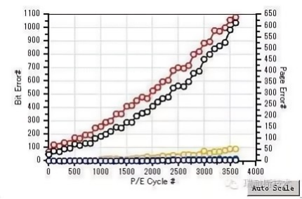
1. Bit Error caused by write/erase operation can be by testing RBER and UBER, tests to the NAND flash can be done in the order of “Erase->Write->Comparison”, the change of RBER can tell the real durability of the NAND Flash.
The detail tests to RBER and UBER as follows: NFA100-E can obtain data of RBER and UBER through simple settings (e.g. set 4 sets of ECC with different codeword length for reference).
The following test results means: The RBER of this MLC NAND Flash is 10^(-5.821), UBER is 0 (Because few P/E cycle was done), generally SSD requires the UBER of above 10^(-15), whether to reach or exceed 10^(-15) primarily depends on the capability and algorithm of ECC.
.png)
2. ProgramDisturb is normally generated by too high or too low Vpass, invalid capacitive coupling and excessive writes. Suppose programming "11" to “10”, 16V voltage is required for programming Lower Page, while the adjacent Cells may finally receive the effect of 19V, why such phenomenon happens?
Program actually adopts the method of Incremental Step Pulse Programming (ISPP as the abbreviation). Because of the different status of each cell, maybe applying voltage for only one time can finish Program for cells in very good condition. However for cells in bad condition, it may require for increasing voltage to finish Program, the increased voltage value will be divided into several substeps, add a little voltage every time, then use Vread to judge whether the target voltage is achieved or not, e.g. Vread is 20V, then the voltage applied to the Upper Page of "10" should not exceed 19V (Vread>Vth), suppose adding 200mV at each step from the normally needed 16V to 19V, then it needs 15 times to finish Program. In the worst case, such phenomenon actually results in the affect to adjacent cells by 19V, data error is more likely to happen, some “Bad” cells may infect their neighbors to “Bad” cells too.
The method of testing Program Disturb is quite easy, we just need to do basic and normal operations including Erase, Program and Read to the specified Block, and NFA100-E can draw conclusions quickly.
3. DataRetention Error
Two reasons may cause Data Retention Error:
a. The root cause of Data Retention Error is TDDB (Time Dependent Dielectric Breakdown) of FG leads to the increase of leakage current at the low electric field, and then the increase of leakage current weakens the cell’s transfer ability of saving the threshold voltage, sequentially results in Data Retention Error.
b. Another reason causes Data Retention Error is what mentioned above, the operations of Erase and Program cause oxide layer collect electric charge, this affects the threshold voltage of the cell, when the electric charge detraps, threshold voltage shifts and Bit reverses.
Theoretically, if the voltage of the cell completely lost (lower than 0V), the final result of Data Retention Error is the data in this cell turns to “11”, i.e. “10”, “01”, “00” turn to “11” eventually.
We can refer to JEDEC standard for the method of testing Date Retention, NFA100-E provides 2 test methods:
a. Directly use Data Retention interface to test step by step (refer to the following picture).
b. Test the Error Rate. First do 1000 P/E cycles to the NAND Flash by NFA100-E under room temperature and write a pseudo-random number, then put the NAND Flash into the temperature chamber of 120°C and take it out after 34’13”, verify the Error Rate using the Read Only mode of NFA100-E, no Error Rate occurs after this test cycle indicates the Data Retention of 1 year. Repeat this cycle, the number of test cycles before Error Rate occurs means the Data Retention years.
.png)
4. ReadDisturb
Read operation may cause errors to adjacent cells as well, the reason is read operation applies 0V voltage to the selected page and 5V to the unselected pages, and whether there is current flow from source to drain electrode determines whether the cell is “1” or “0”, current flow exists means the threshold voltage of the cell is lower than the applied voltage and data is “1”, no current flow indicates the threshold voltage of the cell is higher than the applied voltage and data is “0”. Therefore, read operation causes program operation in some sense to unselected cells and lead to the increase of the threshold voltage, thus results in bit reverse.
.png)
The Influence to Error Rate by Temperature
High and low temperature impacts the Error Rate a lot, and according to my test, low temperature does more impacts to the Error Rate than high temperature, the following picture shows the Error Rate of a MLC flash with RBER of 10^(-5.902) under room temperature of 20°C is 10^(-5.259) under -45°C.
.png)
And the Error Rate of this same MLC flash is 10^(-5.683) under +120°C.
.png)


